Generating Composite Video with an STM32 ARM Device
This page contains details of how you can generate (standard-definition) monochrome composite video using just an STM32 ARM device and a simple video/sync combiner circuit. I came up with the idea 2 weeks ago and once I'd thought of it, I was like a dog with a bone... Having completed the composite video implementation I then made modifications for 640x480 VGA on a standard PC monitor; see the bottom half of this page·
Basic Concept
The video stream is output using a SPI port fed by a circular DMA. Horizontal syncs are generated using a timer and vertical syncs from a second timer clocked by the first timer.
My initial thought was to use the onboard DAC (in 8 bit mode) to output composite video and syncs directly, as I had done this some 15 years ago on a DSP board with a high-speed DAC. Unfortunately, the DACs built into the STM32 series do not have sufficient sample rate throughput and signal bandwidth. The on-chip 'buffer amplifier' makes things even worse bandwidth-wise and should be turned off. Even then, the DAC fails to deliver alternating high/low samples at 1Msps. An ST application note (AN4566) suggests the best one can hope for is to disable the onboard buffer and provide your own external, current-mode buffer amplifier. Even then, you'll be lucky to reach 2MHz bandwidth on the STM32F446 that I was planning to use.
So my next plan was to use a QSPI port to deliver 4, parallel bit-streams into an external R2R DAC and buffer. I gave up on this too, as the STM documentation implies that the QSPI port is designed ONLY for talking to external memory devices and is incapable of simple data streaming. That said, I may revisit this again at some point in case there is a way to disable the hardware-protocol baked in to the QSPI peripheral.
So, that leaves the conventional SPI port. This can be used as a parallel to serial converter to deliver 1-bit video. Fortunately, this works perectly.
Design Details
I have used an STM32F446RET Nucleo64 board. The STM32 clock tree is configured with APB1 peripheral clock (for SPI) at 45MHz and APB2 timer clock (for TIM1) at 180MHz. I have used the 8MHz 'external clock' provided by the STLINK part of the Nucleo64 board, as this has a real crystal and is significantly more stable than the STM32's internal RC oscillator, which I tried first and experienced horrible video jitter.
The SPI port bit clock is set to 11.25MHz and with video timings broadly similar to PAL, one can achieve 480 visible pixels in a line totalling 704 clocks. I did try a SPI bit clock of 15MHz which yielded 640 visible pixels in a line totalling 960 clocks but concluded that 15MHz is just too fast for normal video monitors (7.5MHz alternating pixel frequency, where a typical TV monitor's bandwidth would be less than 6MHz).
Timer TIM1 is set to deliver line syncs of around 4.7us duration using PWM mode 1, prescale 7, reload 703, pulse width 52 and output trigger OC1. Timer TIM2 is set to use TIM1 as its clock input (trigger source ITR0) and to provide a field of 312 lines. The field sync is 6 lines wide. TIM2 is in PWM mode 1, prescale 0, reload 311 and pulse 5. The video output is not interlaced.
The SPI port and timers are started once in software and left to run indefinitely as background 'tasks'. Since the SPI is fed constantly by a circular DMA, the buffer needs to hold data for every pixel in the field, including those in the sync and porch intervals. The total DMA buffer is therefore 704x312 pixels, or 27456 bytes. It is the job of the video plotting routines to access only the correct pixels within this buffer.
Video and Sync Combiner
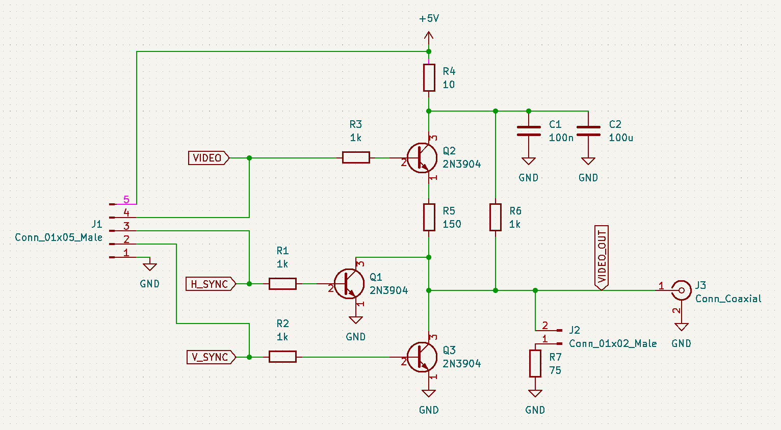
This curcuit requires the video signal and both sync signals to have +ve polarity. The polarity of the timer outputs can be configured appropriately within the peripheral registers.
With all 3 transistors off, the video output line (into a 75ohm load) is biassed at around +0.3V by R6. This provides the black level. The video signal from the ARM will swing between ~0 and ~3.3V. Emitter follower Q2 allows this to lift the video output line up to ~1V. When either of the sync inputs is high, open collector transistors Q1 or Q3 drag the video level down to ~0V (sync level). The jumper-selectable 75ohm resistor is provided for easy testing without a 75 ohm load connected.
Sample Images
These images were captured from an ancient 9" B&W monitor. This gives significantly better image quality than a colour TV as it has no shadow-mask and no comb filter:
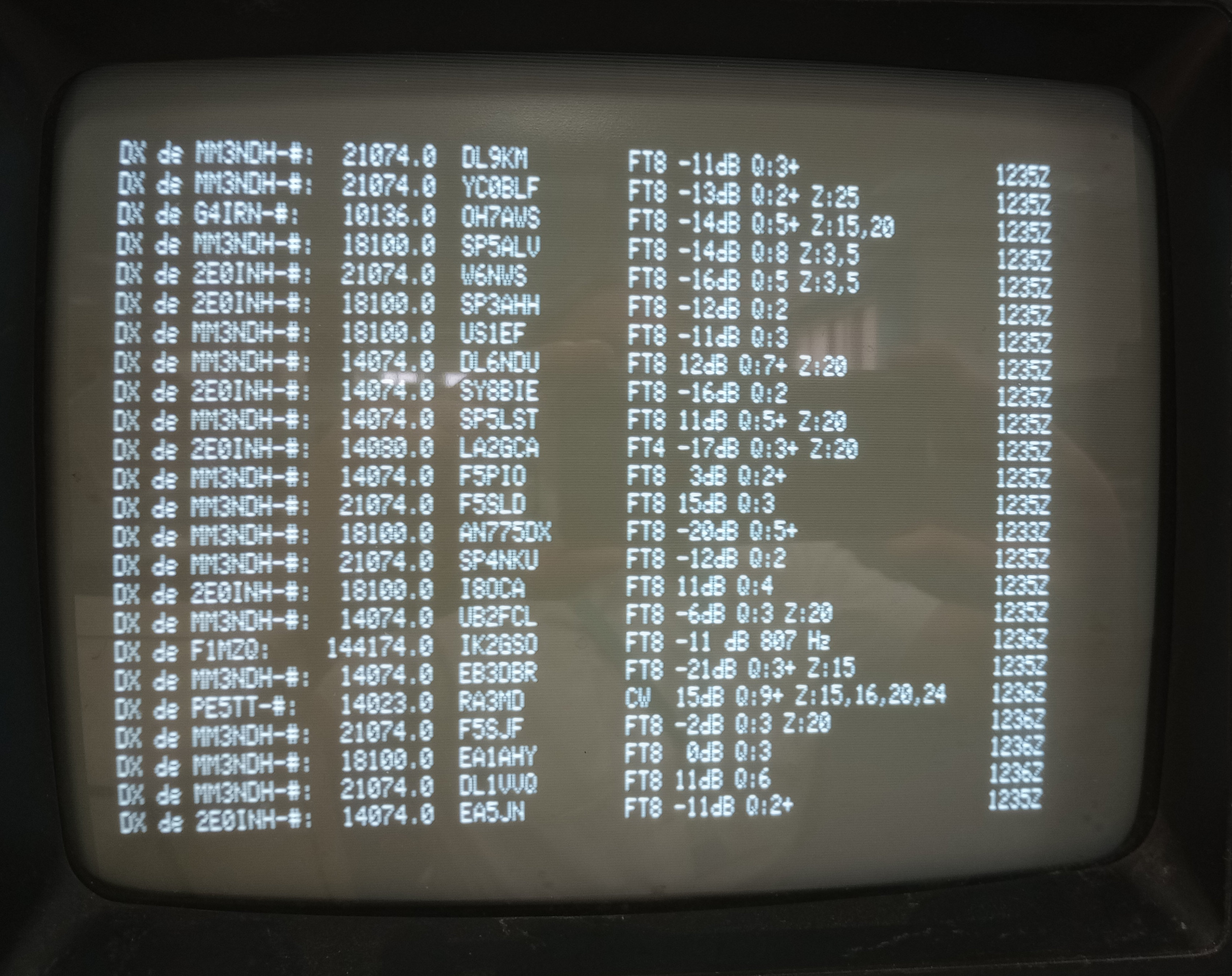
80 x 24 text showing live Reverse Beacon Network data from the DX cluster:

To achieve 80 x 24 text with a pixel resolution of 480 x 240, a 5 x 8 pixel font in a 6 x 10 character-cell must be used. (This is relatively complicated to plot into the framebuffer when compared to an 8 x 8 pixel font, which would align naturally with the bytes in the frame buffer):
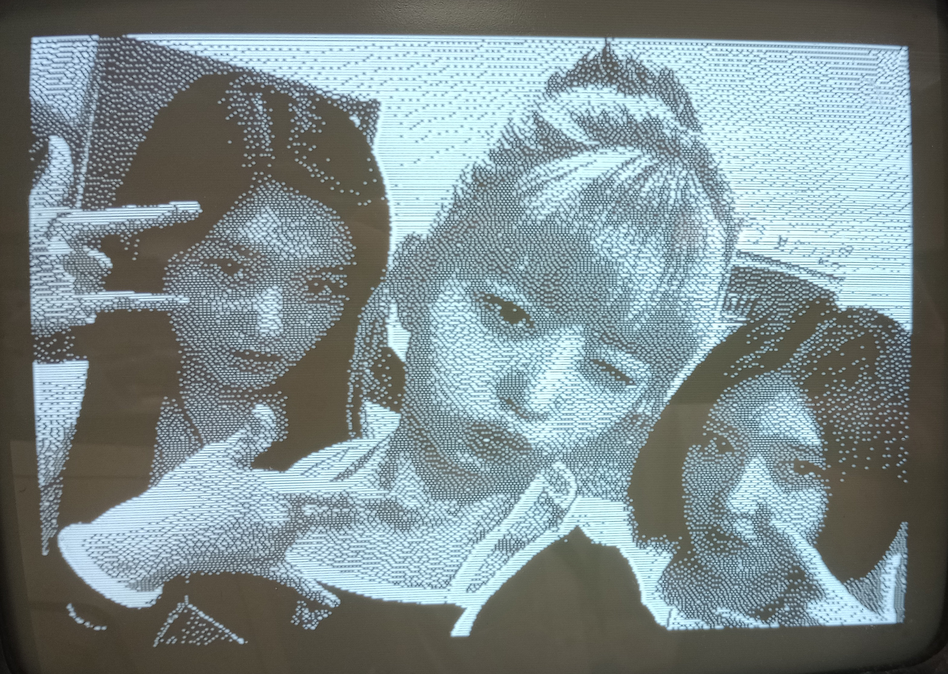
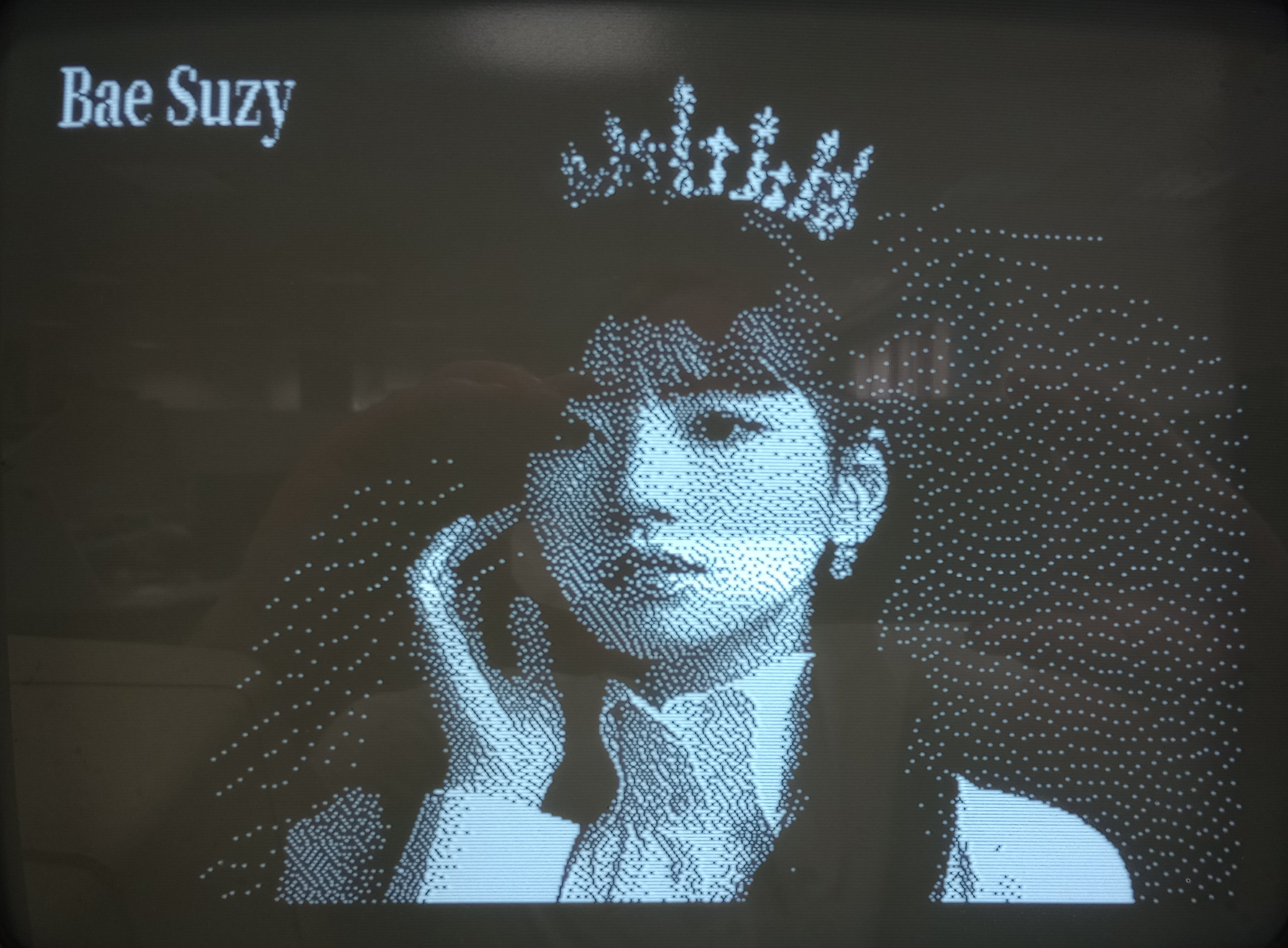
Various 480 x 240 pixel images of KPop girls using error-diffusion dithering to represent greyscale:

Generating VGA Video
Shortly after completing the standard-definition composite video project, I realised that (monochrome) VGA video might be within reach if I can get a pixel clock of 25MHz working. The STM32F446 chip that I am using specifies a maximum AHB1 peripheral clock rate of 45MHz and given that the SPI port has a minimum prescale division of 2, would only yield 22.5MHz. As it happens, even though the STM CubeMX clock tree designer complains if I specify an AHB1 clock of 50MHz, it allows code generation to proceed. Alternatively, if you are setting up the clock tree manually you can also achieve an AHB1 clock of 50MHz.
With an SPI pixel clock of 25MHz (0.7% slow WRT official VGA pixel clock of 25.175MHz), all that was needed was to adjust the video timings in the code and to build a different video output buffer. I reintroduced code to plot an 8x8 bitmap font and added code to plot an 8x12 VGA-style font.
VGA Video Driver
The H and V sync inputs on PC monitors are seemingly still 'TTL'-style signals. I found this somewhat hard to believe, given that a low source/output impedance and high load/input impedance are not compatible with 75ohm coaxial cables, which appear to be used within VGA monitor cables. (That said, I have seen VGA cables where the RGB signals are coaxial and the sync and sense/data lines are twisted pairs.) Either way, it means that the GPO pins from the STM32 can drive the sync lines directly without the need for buffering. I have a 240ohm series resistor between each GPO pin and the cable to provide some pin protection and to reduce edge ringing.
For the RGB video feed, I connect all 3 RGB lines together at the VGA connector. This results in white pixels but presents a load of 25ohms. A single NPN emitter follower is used to drive this load, with a 470ohm base resistor, +5V on the collector and a 62ohm emitter resistor.
Sample VGA Images
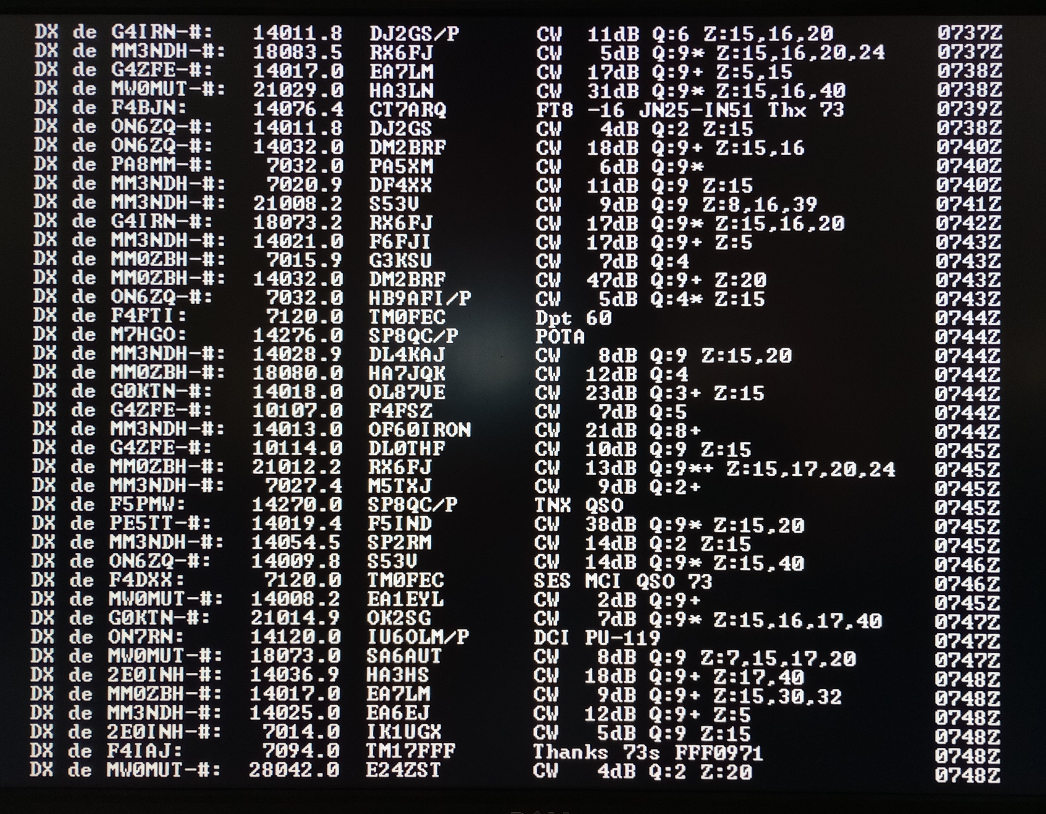
80 x 40 text using 8x12 character cell, showing live Reverse Beacon Network data from the DX cluster:
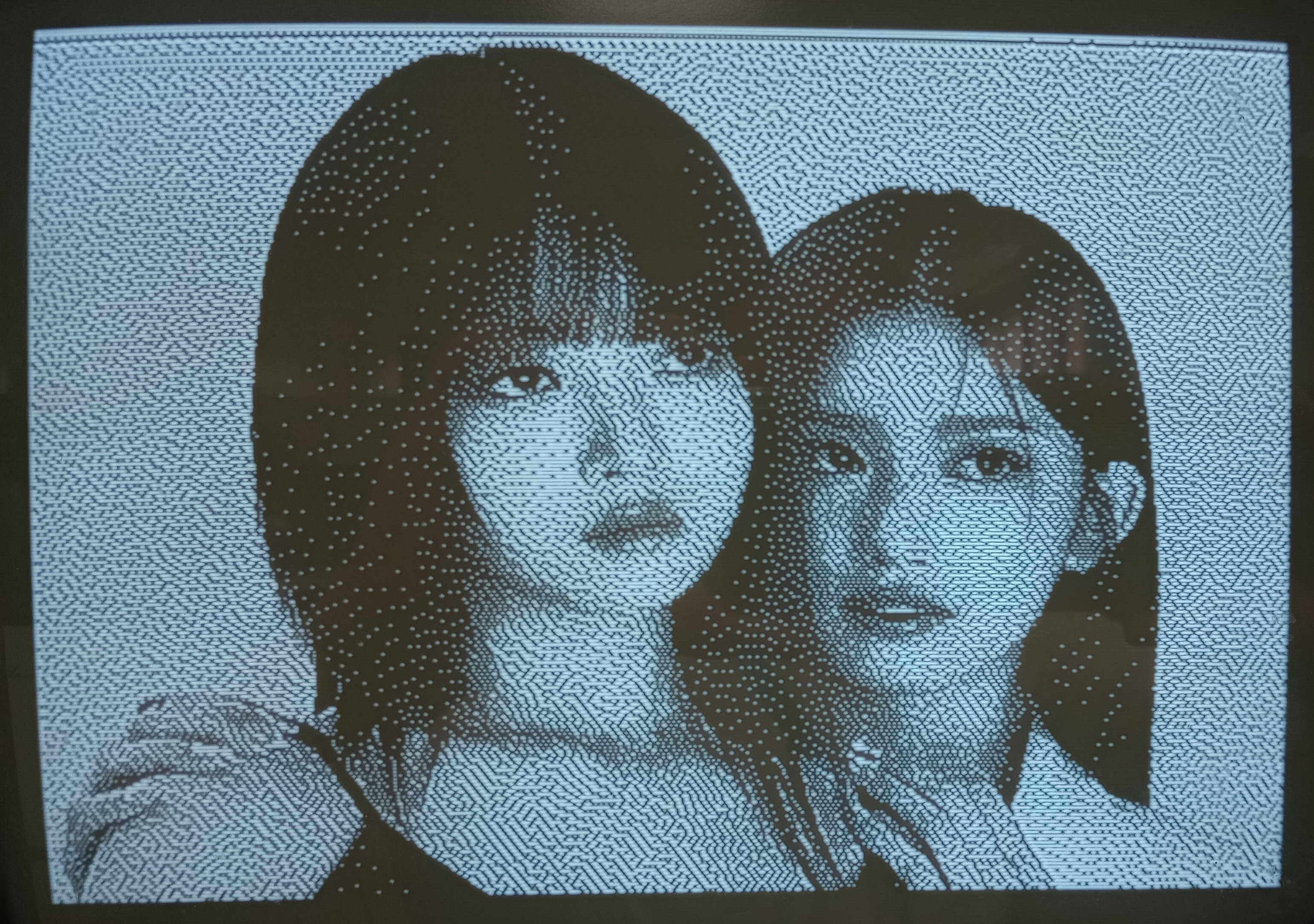
Various 640 x 480 pixel images of KPop girls using error-diffusion dithering to represent greyscale:


